The key to surviving component shortages is not stockpiling parts, but embedding resilience directly into the PCB architecture itself.
- Flexible designs accommodate multiple component footprints and thermal profiles, turning supply chain volatility into a manageable variable.
- System-level strategies like hardware abstraction decouple software from specific silicon, future-proofing the entire product.
Recommendation: Shift your design philosophy from optimizing for a single, perfect BOM to creating a robust platform that validates and accepts a range of pre-approved alternative components.
For electrical engineers and product designers, the global chip shortage has transformed PCB design from a predictable process into a high-stakes exercise in crisis management. The frustration of seeing a meticulously crafted design halted by a single unavailable microcontroller or power IC is a shared pain point across the industry. Standard advice often revolves around logistical solutions: diversifying suppliers, placing bulk orders, or redesigning on the fly. While practical, these are reactive measures that treat the symptoms, not the cause.
The common approach focuses on managing the procurement of a fixed Bill of Materials (BOM). But what if this entire premise is flawed in an era of unprecedented supply chain volatility? The real source of fragility lies in designs that are intrinsically locked to specific part numbers, with no built-in tolerance for substitutes. This creates a brittle system where a single point of failure can cascade into months of delays and costly respins.
This article proposes a fundamental shift in perspective. Instead of reacting to shortages, we must design for them. The true path to immunity lies in treating the PCB not as a static carrier for one ideal set of components, but as a flexible, resilient platform engineered to absorb component variability. It’s a move from designing a product to designing an architecture.
We will explore this strategic philosophy through a series of deep dives, from the material science of thermal management and advanced Design Rule Checking (DRC) to the architectural principles that allow automotive ECUs to remain agile. This guide provides the engineering methodologies to build resilience into the very copper of your next design.
This guide breaks down the core strategies for building supply-chain-resilient PCBs. The following sections detail the critical engineering decisions that move a design from fragile to robust.
Summary: Designing for Disruption: A Guide to Shortage-Proof PCBs
- Why Overheating PCBs Cause 50% of Field Failures in Compact Devices?
- How to Use DRC Checks to Prevent Costly Manufacturing Respins?
- FR-4 vs Metal Core: Which Material Is Essential for High-Power LED Circuits?
- The Routing Error That Destroys High-Speed Data Transmission
- When to Switch from Hand Soldering to Pick-and-Place Assembly?
- How to Redesign Car ECUs to Accept Available Chips?
- Why Manufacturers Glue Batteries to Make Repair Impossible?
- How to Validate a Motherboard Design Before Committing to Mass Production?
Why Overheating PCBs Cause 50% of Field Failures in Compact Devices?
The global chip shortage forces engineers to substitute components, often with parts that have different thermal characteristics. This reality makes thermal management the first line of defense against product failure. When a substitute chip runs hotter or has a different thermal expansion rate, it introduces mechanical stress on the board and its connections. This isn’t a minor issue; research shows that nearly 60% of electronic product failures can be traced back to solder joint issues, many of which are initiated or accelerated by thermal stress.
The core of the problem lies in the Coefficient of Thermal Expansion (CTE) mismatch. Every material on a PCB—the laminate, the copper, the component leads, the solder—expands and contracts at a different rate when heated. In a well-designed system with the intended components, these differences are accounted for. However, when a shortage forces the use of an alternative component, its different CTE can create immense mechanical stress during thermal cycling (the heating and cooling that occurs during normal operation).
Case Study: Consumer Electronics Thermal Cycling Failure
A batch of consumer devices experienced intermittent power failures. The root cause was cracked solder joints on critical power components. Analysis revealed that under thermal cycling (-10°C to 85°C), the joints failed due to CTE mismatch between the FR-4 PCB (14 ppm/°C) and the component leads (24 ppm/°C). The original design relied on a specific component with a closer CTE match. The forced substitution, combined with insufficient solder volume, led to catastrophic field failures. The solution involved not just finding another part, but redesigning the assembly process with a 20% increase in solder paste and a new reflow profile to withstand the higher mechanical stress, demonstrating that resilience requires adapting the process, not just swapping parts.
Therefore, designing for shortage immunity means designing with thermal headroom. This involves selecting substrate materials and employing layout techniques (like thermal vias and copper pours) that can handle not just the ideal component’s heat, but also the potential “worst-case” thermal profile of a future substitute. This proactive approach prevents a supply chain problem from becoming a reliability disaster.
How to Use DRC Checks to Prevent Costly Manufacturing Respins?
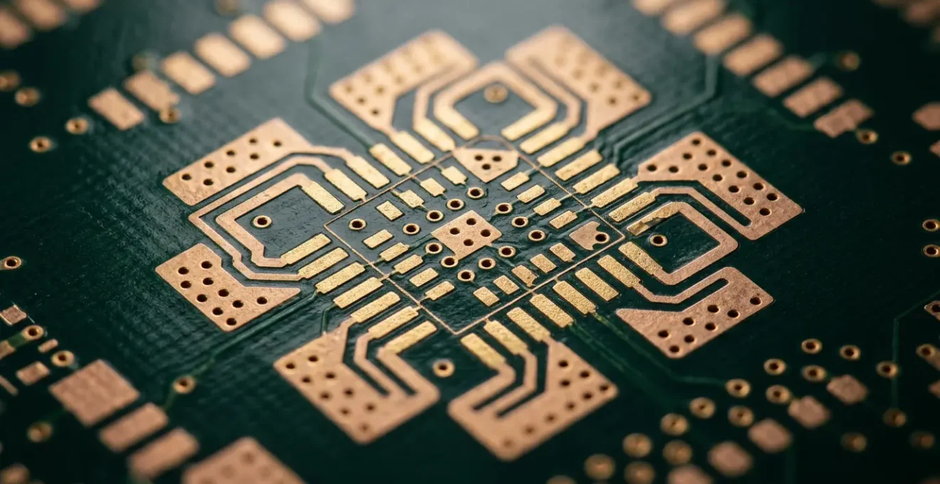
Design Rule Checks (DRC) are a standard part of PCB design, but in the context of component shortages, their role evolves from a simple manufacturability check to a strategic validation tool for supply chain resilience. A typical DRC run ensures a single, ideal BOM can be manufactured. A supply-chain-aware DRC strategy, however, must validate that the board can accommodate a *range* of potential components. Failing to do so can lead to devastatingly expensive board respins; research shows the average cost of a PCB respin reaches nearly $28,000, a cost that can cripple a project budget.
To prevent this, engineers must move beyond the default rule sets provided in their EDA software. The goal is to create a “virtual kit” validation process where the layout is checked against the constraints of multiple components and even multiple contract manufacturers (CMs). This involves creating custom rules for multi-footprint pads, which can accommodate, for example, both a QFN and an SOIC package for the same functional block. It also means running DRCs against the specific rule sets of several potential CMs to ensure the design is portable and not locked into a single fabricator’s capabilities.
As the visual above suggests, this is a layered validation process. It’s no longer about a single “pass/fail” but about confirming the design’s flexibility across multiple manufacturing and component scenarios. This proactive validation is the difference between a robust, manufacturable design and one that is perpetually one component shortage away from a complete redesign. The most effective approach is to enable continuous online DRC, catching violations as they occur during layout, rather than facing hundreds of errors right before fabrication.
Action Plan: 5-Step DRC Strategy for Supply Chain-Aware Validation
- Create custom DRC rules for multi-footprint layouts: Validate solder paste conflicts, silkscreen overlaps, and acid trap risks specific to flexible QFN/SOIC package combinations.
- Configure BOM variant checks in your EDA tool: Automate verification that each alternative component (Part A vs. Part B) meets manufacturing constraints, not just the primary choice.
- Set up manufacturer-specific rule sets: Run DRCs against component libraries and footprint recommendations of 2-3 potential contract manufacturers to ensure design portability.
- Enable continuous online DRC during layout: Catch violations immediately during placement and routing to prevent the accumulation of hundreds of errors.
- Run comprehensive batch DRC before fabrication: Perform final validation of all enabled rules, including computationally expensive checks, before generating Gerber files.
FR-4 vs Metal Core: Which Material Is Essential for High-Power LED Circuits?
The choice of PCB substrate is a foundational decision that directly impacts a design’s thermal resilience. While standard FR-4 is ubiquitous and cost-effective, it is a poor thermal conductor. For high-power applications like LED lighting or motor drivers, relying on FR-4 without significant thermal mitigation strategies is a recipe for failure, especially when component substitutions may introduce parts with higher thermal dissipation. The alternative, a Metal Core PCB (MCPCB), integrates a layer of aluminum or copper that acts as a highly efficient heat spreader, dramatically lowering component operating temperatures.
The strategic trade-off is no longer just about performance versus cost; it’s about resilience versus risk. An MCPCB offers superior thermal headroom, making the design far more tolerant of substitute components that might run hotter than the original spec. While the upfront cost is higher, it acts as an insurance policy against production halts or field failures caused by thermal overloads. The following table, based on a recent comparative analysis of thermal performance, breaks down the strategic considerations.
| Design Criterion | FR-4 with Thermal Vias | Metal Core PCB (MCPCB) | Hybrid Strategy |
|---|---|---|---|
| Thermal Conductivity | 0.3-0.4 W/m·K (base laminate) | 1.0-8.0 W/m·K (aluminum core) | Localized MCPCB module in FR-4 carrier |
| Component Flexibility | High – supports standard assembly | Moderate – limited to TH or special SMT | High – FR-4 areas accept all packages |
| Upfront Cost | Low ($50-200 for prototype) | High ($200-500 for prototype) | Moderate ($150-350 with modular design) |
| Shortage Resilience | Good – thermal headroom allows substitute parts with higher TDP | Excellent – can handle extreme thermal variance | Excellent – isolates high-risk components |
| Production Halt Risk | Moderate – entire board redesign if thermal limits exceeded | Low – superior thermal management prevents failures | Very Low – only small module needs redesign |
| Design Complexity | Moderate – requires careful thermal via placement | High – special design rules for metal core | High – requires modular architecture planning |
The “Hybrid Strategy” represents a sophisticated approach to resilience. By designing a small, high-risk section of the board (e.g., the power stage) as a modular MCPCB that mounts onto a larger FR-4 motherboard, engineers can isolate the most volatile components. If a critical power IC becomes unavailable and its only substitute requires superior thermal management, only the small, less expensive module needs to be redesigned, not the entire motherboard. This modular architecture embodies the principle of designing for interchangeability at the material level.
The Routing Error That Destroys High-Speed Data Transmission
In high-speed digital design, signal integrity is paramount. Even minor deviations in trace impedance can corrupt data, leading to jitter, crosstalk, and complete system failure. The chip shortage has amplified this challenge tenfold. When an engineer is forced to substitute a high-speed component like an FPGA or a memory chip, the new part may have a slightly different die capacitance or pinout, which can detune the carefully calculated impedance of the transmission lines. Simply swapping the part without re-validating the routing is a critical error.
A common failure mode occurs when a design’s trace impedance is mismatched. For example, a 10 Gbps signal requiring a 50-ohm trace that is inadvertently routed at 55 ohms will suffer from reflections and degradation. This can happen due to inconsistent dielectric thickness in the PCB stack-up or, more relevantly today, because a substitute component’s electrical characteristics were not accounted for in the original impedance calculation. This highlights a core tenet of resilient design: routing must be planned not just for one component, but with enough margin to accommodate the characteristics of potential substitutes.
This reality is a direct consequence of a fragile design philosophy. As the engineering community often laments, the biggest mistake is designing for a single part number without a contingency plan. The following insight from a discussion among electronics engineers captures this sentiment perfectly:
The biggest single mistake engineers make is designing around a specific part number without considering what happens if that part becomes unavailable.
– Electronics engineering community, Forum for Electronics – How to Design Your PCB to Survive Component Shortages
The solution is to design for interchangeability at the layout level. This means using universal footprints where possible, but more importantly, performing sensitivity analysis. Engineers should model how impedance and signal integrity are affected by the range of capacitances and timings specified across all pre-approved alternative components in the BOM. This ensures the final routing is robust enough to maintain performance, regardless of which specific chip is available on assembly day.
When to Switch from Hand Soldering to Pick-and-Place Assembly?
In the prototyping and small-batch production phases, hand soldering can seem like a flexible and low-cost option. However, in an era of component volatility, this manual process becomes a significant liability. The consistency and precision required to reliably place modern surface-mount packages (like QFNs or BGAs) and manage multi-footprint layouts are nearly impossible to achieve by hand, especially when dealing with a rotating cast of alternative components. A switch to automated Pick-and-Place (P&P) assembly is not just a matter of scale; it’s a strategic decision for ensuring quality and manufacturability.
The speed at which the component market can change makes this transition critical. As the engineering team at Treetown Tech noted, the stability of the supply chain is an illusion.
50,000 in-stock chips can vanish in a single day and be replaced with a 99+ week lead time.
– Treetown Tech engineering team, PCB Design in a Chip Shortage – Treetown Tech
This level of volatility means a design must be validated for automated assembly from the very beginning. Relying on hand soldering for prototypes creates a false sense of security; a design that works when painstakingly assembled by a skilled technician may fail completely on a P&P line, especially with alternative parts that have slight variations in size or lead coplanarity. Automated assembly provides the process control needed to manage these variations, ensuring consistent solder paste deposition, accurate placement, and repeatable thermal profiles in the reflow oven.
Therefore, the decision to switch to P&P should be made as early as possible. Even for prototype runs of 10-25 units, using a CM with P&P capabilities is a vital validation step. It stress-tests the design’s manufacturability with the real-world equipment and processes it will face in mass production. This investment upfront prevents the disastrous discovery that your “finished” design is, in fact, unmanufacturable at scale with the components you were forced to procure.
How to Redesign Car ECUs to Accept Available Chips?
The automotive industry, one of the hardest hit by the chip shortage, offers a powerful lesson in architectural resilience. A modern Electronic Control Unit (ECU) is a complex system, where a single unit for functions like engine management or advanced driver-assistance systems (ADAS) can depend on hundreds of different microcontrollers, transceivers, and sensors. The traditional approach of tying the ECU’s software directly to a specific MCU model proved disastrously fragile when those MCUs became unobtainable.
The strategic solution adopted by leading automotive designers is the implementation of a Hardware Abstraction Layer (HAL). This is a software engineering principle, often standardized through frameworks like AUTOSAR (Automotive Open System Architecture), that creates a buffer between the high-level application code and the low-level hardware. Instead of writing software that “talks” directly to the registers of a specific NXP microcontroller, for example, the software talks to the generic AUTOSAR interface. This makes the application code portable.
This modularity, as conceptualized in the image above, is the key. If a specific MCU becomes unavailable, engineers can substitute it with a different one from STMicroelectronics or Renesas. The only software that needs significant changes is the small, targeted set of drivers that make up the HAL for that new chip. The core application logic—representing thousands of hours of development and validation—remains untouched. As the Siemens engineering team explains, this architectural choice is fundamental to agility.
Software developed to the AUTOSAR standard is highly portable and interfaces to the silicon through layered software, enabling developers to verify and validate a substantial amount of their software independently from underlying MCU hardware details and differences.
– Siemens engineering team, Global microcontroller shortage on ECU software development white paper
This is the ultimate expression of designing for interchangeability. It moves beyond flexible footprints to a truly modular and abstract system architecture where the PCB and its software are not dependent on a single, irreplaceable part. It’s a lesson from which all electronics designers can learn, regardless of their industry.
Why Manufacturers Glue Batteries to Make Repair Impossible?
The practice of gluing batteries into consumer electronics, making them difficult or impossible to repair, is often seen as a symbol of planned obsolescence. While driven by goals of sleek design and simplified assembly, it represents a deeper design philosophy: one that prioritizes initial form and cost over long-term serviceability and adaptability. This exact same philosophy of “designing for lock-in” is at the heart of the supply chain crisis when applied to component selection. A design built around a single-source, non-replaceable microcontroller is the engineering equivalent of a glued-in battery.
Both represent a fragile design philosophy. They create a product that is highly optimized for one specific set of circumstances (a specific battery model, a specific MCU part number) but which shatters when those circumstances change. The global chip shortage, which analysis found has impacted at least 169 industries, exposed this fragility on a massive scale. Designs that were considered “optimized” were revealed to be brittle, unable to adapt when their single-source linchpin component vanished from the market.
As a consensus in the PCB design community suggests, this approach is a strategic dead end. Tying a product’s fate to a single, unique component is a critical vulnerability. The resilient alternative is to embrace a philosophy of modularity and interchangeability. This means treating critical components not as permanent fixtures, but as replaceable modules. This might involve using standardized daughterboards for processors, designing with multi-footprint layouts, or implementing the hardware abstraction layers seen in the automotive industry.
By consciously rejecting the “glued-in battery” mindset, engineers can create products that are not only more resilient to supply chain disruptions but are also more sustainable and serviceable over their entire lifecycle. It is a strategic choice to prioritize adaptability over initial optimization, a choice that pays massive dividends in a volatile world.
Key Takeaways
- Thermal Headroom is Non-Negotiable: Design your PCB’s thermal management system to handle the worst-case substitute component, not just the ideal one.
- Validate for Variants, Not Just One BOM: Use advanced DRC and simulation to ensure your design is manufacturable with a range of pre-approved alternative parts and across multiple CMs.
- Embrace Architectural Abstraction: Decouple your application software from specific hardware using Hardware Abstraction Layers (HALs) to make your core logic portable across different MCUs.
How to Validate a Motherboard Design Before Committing to Mass Production?
The final and most critical step in creating a shortage-proof design is validation. A design that is theoretically flexible is worthless until that flexibility has been rigorously tested. Committing to mass production without this validation is a gamble, especially in a market where future volatility is a certainty. For instance, with AI driving demand, analysts predict a potential 30% price increase in memory chips in late 2024, forcing even more substitutions. Traditional validation, which tests if the ideal-BOM prototype works, is no longer sufficient. The new paradigm is to validate for chaos.
This means adopting a “chaos engineering” approach to hardware prototyping. Instead of building a “golden” prototype with all the best-case components, the goal should be to build “Frankenstein” prototypes. These are boards intentionally populated with the least desirable, but still in-spec, alternative components from your approved list. This stress-tests the design’s margins and exposes weaknesses that would never appear in an ideal-case scenario. Does the board still meet its thermal requirements with the hotter-running power IC? Does it pass signal integrity tests with the MCU that has a slightly higher pin capacitance?
This validation must also extend to manufacturing partners. Running small, parallel validation builds with two or three different contract manufacturers is essential. This tests the portability of your design data and uncovers any CM-specific process limitations before you are locked into a single supplier. The process should be data-driven, with engineers meticulously documenting failure modes by component variant. This builds a powerful institutional knowledge base, creating a matrix that shows which alternative parts cause which issues, informing and de-risking future designs.
Ultimately, this rigorous, multi-variable validation process is the final gatekeeper. It transforms the principles of resilient design from theory into a proven, production-ready reality. It is the definitive confirmation that the board is not just designed to work, but designed to survive.
By embedding these strategic principles of thermal headroom, interchangeability, abstraction, and rigorous validation into your engineering workflow, you can move from a reactive posture of fighting shortages to a proactive stance of designing for disruption. The next step is to apply this resilient design philosophy to your very next project.