The goal of motherboard validation is not to confirm that a prototype works, but to systematically discover all the ways it will fail in the field.
- Most prototype failures are not catastrophic “no-boot” issues, but latent defects (e.g., from ESD or power noise) that cause unpredictable field failures later.
- The fidelity of your test setup is critical; a plastic 3D-printed enclosure can invalidate all thermal and RF testing, unlike a CNC-machined metal prototype.
Recommendation: Shift from a sequential checklist to a “Parallel Path” validation strategy, where manufacturing resilience and testability are engineered into the design from day one.
For a hardware startup, the Engineering Validation Test (EVT) phase is a moment of truth. The first prototypes are back from the assembly line. The question on everyone’s mind is simple: “Will it boot?” While a successful power-on is a crucial milestone, focusing solely on it is a strategic error. The industry is littered with products that passed their initial tests but failed catastrophically in the hands of customers. Many teams believe validation is about running a series of functional tests, checking signal integrity, and performing basic thermal analysis.
This approach often overlooks the most dangerous threats: latent failures. These are subtle weaknesses in the design—microscopic ESD damage, marginal power integrity, or unforeseen component interference—that don’t cause immediate failure but create a product that is unstable, unreliable, and destined to fail prematurely. These are the issues that lead to costly recalls and damage a startup’s reputation beyond repair. Analysis shows that while a prototype might seem complete, it often represents a fraction of the real work needed for a robust, manufacturable product.
But what if the true purpose of validation wasn’t just to confirm function, but to actively hunt for these hidden weaknesses? This guide reframes the validation process not as a simple checklist, but as a methodical investigation. We will move beyond the pass/fail mindset to adopt the rigor of a detective, employing specific strategies to uncover the subtle clues of future failure before committing to the immense cost of mass production.
This article provides a structured methodology to build resilience into your motherboard design. We will dissect the most common failure points, from power integrity to component placement, and offer concrete strategies for detection and prevention. By the end, you will have a framework to transform your EVT from a simple functionality check into a true test of manufacturing readiness.
Summary: How to Validate a Motherboard Design Before Committing to Mass Production?
- Why Do 30% of First-Run Prototypes Fail to Boot?
- How to Use an Oscilloscope to Find Noise in Power Lines?
- ATX vs Mini-ITX: Which Standard Fits Your Industrial Enclosure?
- The ESD Mistake That Kills Prototypes on the Workbench
- How to Arrange Components to Minimize Interference on Density Boards?
- How to X-Ray Chips to Detect Malicious Modifications?
- 3D Printing vs CNC Machining: Which Is Best for Your Functional Prototype?
- How to Move from Prototype to Mass Production in Under 6 Months?
Why Do 30% of First-Run Prototypes Fail to Boot?
A 30% failure-to-boot rate on a first prototype run is a common, if painful, reality in hardware development. However, this immediate, catastrophic failure is only the tip of the iceberg. The more alarming figure is that, according to industry analysis, up to 90% of electronic products fail to ever reach the market successfully. This disconnect reveals a fundamental misunderstanding of the validation process. The primary cause is not a single design flaw, but a cascade of issues rooted in poor planning, insufficient simulation, and an overestimation of the prototype’s maturity.
Teams fall into the trap of what is known as the “prototype illusion.” A working prototype feels like the finish line is near, but it is merely the starting point for the grueling marathon of validation and manufacturing preparation. As the ByteSnap Design Engineering Team points out, this perception gap is significant.
Your device may appear 80% complete at the prototype stage, but often only represents 10-20% of the work required for production.
– ByteSnap Design Engineering Team, Electronic Product Development: How to Beat the 90% Failure Rate
The reasons for initial boot failure are often tactical: incorrect component footprints, Bill of Materials (BOM) errors, or simple assembly defects. But the reasons for ultimate market failure are strategic. They stem from overlooking Design for Manufacturability (DFM), failing to secure the supply chain for mass production, and underestimating the rigor required for certification (like FCC or CE). A prototype that boots is not a product; it’s a hypothesis that must now be rigorously tested against the realities of mass production and real-world use.
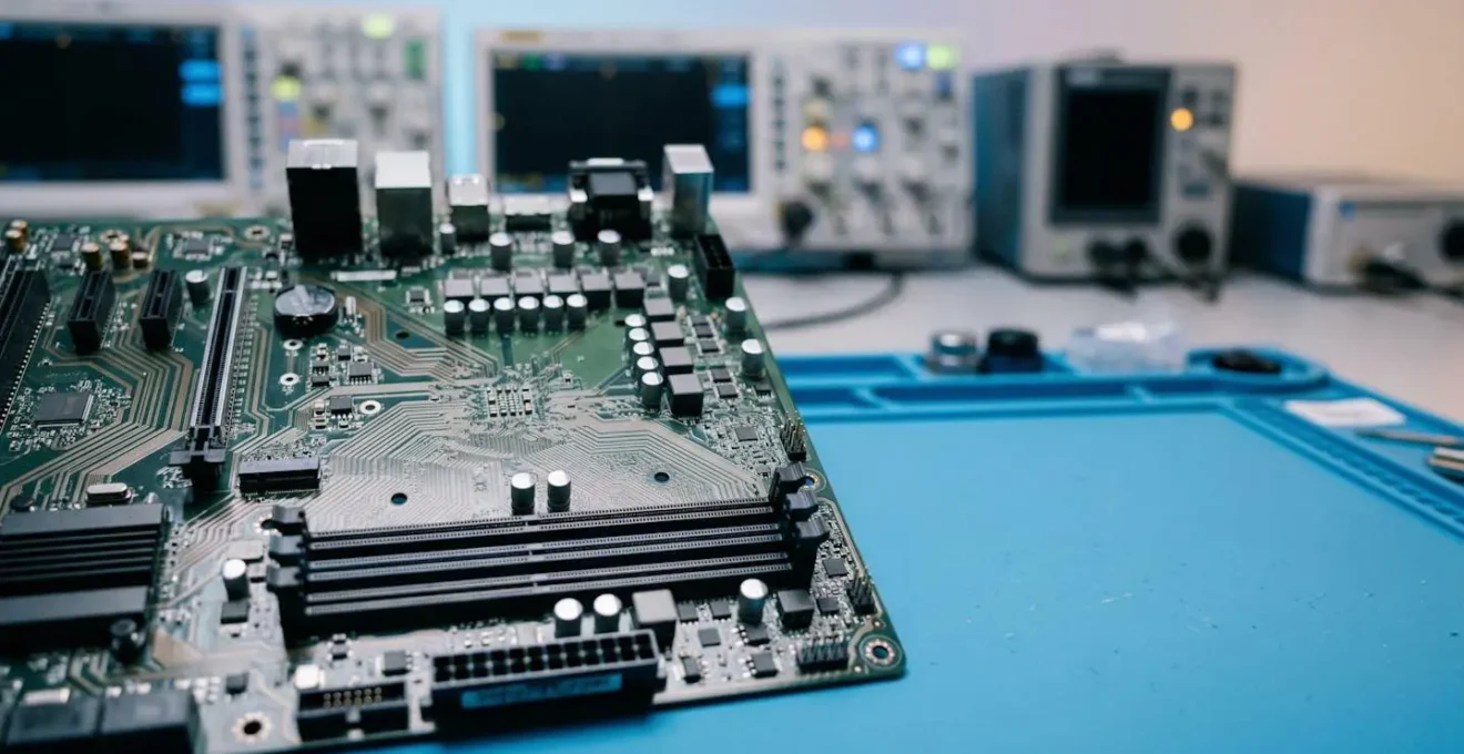
How to Use an Oscilloscope to Find Noise in Power Lines?
Verifying power integrity goes far beyond checking DC voltage levels with a multimeter. A stable 3.3V reading can hide high-frequency noise and transient drops that cause intermittent, hard-to-diagnose system crashes. This is where an oscilloscope becomes an indispensable diagnostic tool, not for what it measures, but for what it allows you to see. The real enemy of a stable system is power supply ripple and noise (PARD), which can be injected by switching regulators, digital components, or external sources.
This macro shot illustrates the precise, physical act of probing a power rail on a dense PCB to hunt for these invisible instabilities.
The standard method is to use the scope in the time domain to look for voltage fluctuations. However, a more powerful technique is to use the scope’s Fast Fourier Transform (FFT) function. FFT converts the time-domain signal (voltage over time) into the frequency domain (amplitude over frequency). This acts like a spectrum analyzer, showing you not just that there is noise, but precisely at what frequencies it occurs. This is a critical forensic tool. For example, a sharp peak at the switching frequency of your DC-DC converter points to inadequate filtering, while broadband noise might indicate a grounding issue.
To effectively find noise, set your oscilloscope to AC coupling with a high-bandwidth limit (e.g., 20 MHz) and a small volt/division setting (e.g., 10-20 mV/div). Use a high-quality probe with a very short ground lead to minimize measurement interference. Probe directly at the power pins of sensitive components like microcontrollers or FPGAs. By analyzing the frequency signature of the noise, you can trace it back to its source and implement targeted solutions, such as adding bypass capacitors or improving the layout, thereby eliminating a major source of latent failures.
ATX vs Mini-ITX: Which Standard Fits Your Industrial Enclosure?
Choosing between motherboard form factors like ATX and Mini-ITX for an industrial product is not just a question of size. While Mini-ITX’s compact 170x170mm footprint is attractive for space-constrained enclosures, this decision has cascading implications for thermal management, I/O expansion, and manufacturing resilience that must be carefully weighed during the design phase.
The first consideration is component density and thermal performance. A Mini-ITX board forces components into close proximity, which can create thermal hotspots and increase electromagnetic interference (EMI). While an ATX board offers more physical separation, allowing for larger heatsinks and better airflow paths, it may be overkill for a dedicated industrial appliance. Your choice must be driven by a thorough thermal simulation based on the power dissipation of your key components, not just the available physical space.
Second is the I/O and expansion ecosystem. ATX boards provide a wealth of PCIe slots, offering maximum flexibility for adding specialized industrial I/O cards. Mini-ITX, typically limited to a single PCIe slot, demands a more integrated design where essential peripherals are placed directly on the board. For a startup, this is a critical trade-off: ATX offers off-the-shelf flexibility at the cost of size and unit price, while Mini-ITX forces a higher upfront NRE (Non-Recurring Engineering) cost for a more compact, application-specific design.
Finally, consider manufacturability and supply chain stability. The ATX standard has a vast, mature ecosystem of enclosures and power supplies, simplifying procurement for early production runs. The industrial Mini-ITX market, while robust, is more specialized. Sourcing long-lifecycle, industrial-grade Mini-ITX motherboards and compatible chassis requires more careful vendor selection. The decision hinges on your product’s specific requirements: if you need extensive, modular I/O, ATX is the safer bet. If a compact, highly integrated, and power-efficient design is paramount, Mini-ITX is the logical choice, provided you account for the increased design and thermal validation complexity.
The ESD Mistake That Kills Prototypes on the Workbench
The most insidious mistake an engineer can make on the workbench is underestimating Electrostatic Discharge (ESD). The common perception of ESD is a visible spark and a component that immediately fails—a catastrophic failure. While these occur, they are not the real threat. The far more dangerous and common issue is latent ESD damage. This is a non-visible, partial degradation of a component’s internal structure caused by a low-voltage ESD event. The component continues to function, passing all initial tests, but is now a “walking wounded” device, destined for premature failure in the field.
This is not a rare occurrence. Rigorous industry studies reveal a startling truth: up to 90% of ESD-related failures are due to latent damage rather than immediate catastrophic events. This means the vast majority of ESD damage is invisible during the EVT phase. The mistake is not just a single accidental zap; it is the systemic failure to maintain a fully grounded ESD-safe workflow for every single interaction with the board. Every touch without a grounded wrist strap, every placement on a non-ESD-safe surface, is a roll of the dice.
Case Study: The “Walking Wounded” Voltage Regulator
A compelling demonstration of this threat comes from Universal Instruments’ Advanced Process Lab. Their research on ESD damage documented a case involving a voltage regulator that was subjected to a minor ESD event. The component passed all immediate functional tests and continued to operate normally for one full hour before experiencing a catastrophic failure. This “walking wounded” phenomenon highlights how hidden damage can lead to unpredictable failures weeks or months later, a particularly grave risk for high-reliability applications in medical or military equipment where failure is not an option.
The only effective countermeasure is uncompromising procedural discipline. This includes using grounded wrist straps, ESD-safe mats, and ionized air blowers, and regularly verifying the integrity of the grounding system. The image below is not just about tools; it’s about the conscious, deliberate process of ensuring a safe handling environment before any contact is made. For a startup, a single latent ESD failure that causes a field return can be an extinction-level event. Prevention is not optional; it is a core principle of professional hardware engineering.
How to Arrange Components to Minimize Interference on Density Boards?
On a densely populated motherboard, component placement is not just a matter of fitting everything in; it is a strategic exercise in managing electromagnetic interference (EMI). Poor placement creates a chaotic environment where “noisy” components pollute “sensitive” ones, leading to system instability, failed compliance tests, and latent field failures. The key to minimizing interference is a methodical approach known as strategic zoning and partitioning.
First, you must classify your components into functional blocks based on their electrical behavior. The primary categories are:
- Noisy Components: These are the polluters. This group includes switching power supplies (DC-DC converters), high-frequency clock oscillators, and high-speed bus drivers.
- Sensitive Components: These are the victims. This group includes analog circuitry (ADCs, op-amps), low-voltage logic, and RF components like antennas and tuners.
- High-Speed Digital: Components like CPUs, FPGAs, and DDR memory fall here. They are both sources and victims of noise.
Once classified, the next step is to create physical “zones” on the PCB. Keep noisy components physically separated from sensitive analog or RF circuits. For example, place the entire power supply section in one corner of the board, and the sensitive analog front-end in the opposite corner. This physical distance is the first and most effective line of defense. Within the high-speed digital zone, ensure that critical traces, like those for DDR memory, are as short as possible and routed with controlled impedance to maintain signal integrity.
Finally, the partitioning must extend to the ground plane. A common mistake is to use a single, unbroken ground plane for the entire board. A better strategy for mixed-signal boards is to create “moats” or splits in the ground plane to isolate the digital and analog ground return paths. This prevents noisy digital ground currents from flowing underneath sensitive analog circuits. By treating component arrangement as a deliberate act of electrical segregation, you can prevent a host of interference problems before they ever arise, building a foundation of stability into your design.
How to X-Ray Chips to Detect Malicious Modifications?
In an era of increasing supply chain concerns, the ability to verify component authenticity is a critical part of hardware validation. 2D and 3D X-ray inspection is a powerful non-destructive technique, but it’s essential to understand its capabilities and limitations, especially when searching for sophisticated hardware Trojans or malicious modifications. The assumption that an X-ray can “see everything” is a dangerous oversimplification.
X-ray inspection excels at detecting package-level and structural defects. It is the go-to method for verifying the quality of Ball Grid Array (BGA) soldering, identifying voids or shorts, and checking the integrity of wire bonds inside an integrated circuit. It can also detect counterfeit components by comparing the internal die size, lead frame, and wire bonding patterns against a “golden sample” from a trusted source. If a chip has a smaller die than expected or a different internal structure, it is a major red flag.
However, X-ray inspection has significant limitations when it comes to detecting modifications at the silicon level. As industry experts clarify, it is only one piece of a much larger puzzle.
X-ray inspection is primarily for die-to-die bonding and package-level inspection, and must be combined with techniques like chemical decapsulation and scanning electron microscopy (SEM) to detect modifications at the silicon level.
– PCB Assembly Industry Experts, Understanding Latent ESD Damage in PCB Assembly
A sophisticated hardware Trojan does not involve changing the package; it involves adding or altering a few logic gates within the silicon die itself. An X-ray does not have the resolution to see these nanometer-scale changes. Detecting such threats requires a multi-stage, destructive process: first, using chemical decapsulation to remove the chip’s packaging and expose the silicon die, followed by imaging with a Scanning Electron Microscope (SEM) to compare the circuit layout layer-by-layer against a trusted design. Therefore, while X-ray is an essential first-pass screening tool for counterfeits and major defects, it should be viewed as the start of a security investigation, not the end.
3D Printing vs CNC Machining: Which Is Best for Your Functional Prototype?
The choice between 3D printing and CNC machining for a prototype enclosure seems like a simple trade-off between speed and cost versus fidelity and strength. While 3D printing (FDM, SLA) is invaluable for rapid ergonomic and form-factor checks, relying on a plastic prototype for full electronic validation can be a critical error. The material properties of the enclosure are not just cosmetic; they are an active component of the system, and using the wrong one can completely invalidate your thermal and RF test results.
The core issue is testing fidelity. A plastic 3D-printed enclosure has vastly different thermal dissipation characteristics than a final production enclosure made of die-cast aluminum or steel. Heat generated by the motherboard will be trapped inside the plastic, leading to artificially high temperature readings and potentially causing you to over-engineer your thermal solution. Conversely, a CNC-machined metal enclosure provides a thermal environment that is much more representative of the final product.
This is not a theoretical concern; it has a direct impact on development cycles and costs, as one research firm discovered.
Case Study: Prototyping Fidelity’s Impact on Validation
In a 2024 hardware development study, InTechHouse demonstrated how enclosure material critically affects validation. When testing military-grade equipment against MIL-STD-810 thermal cycling standards, results from 3D-printed plastic housings were so unrepresentative that they required complete re-validation once the design moved to production metal enclosures. In contrast, CNC-machined aluminum prototypes yielded thermal performance results within 5% of the final die-cast parts. This high-fidelity approach significantly reduced the number of design iteration cycles, accelerating the path to production.
The same logic applies to RF performance. A plastic enclosure is largely transparent to radio frequencies, while a metal enclosure acts as a Faraday cage, affecting antenna performance and EMI/EMC characteristics. Testing your Wi-Fi or Bluetooth radio in a plastic box tells you nothing about how it will perform in its final metal housing. Therefore, the right choice depends on your validation goal. For early-stage fit checks, 3D printing is ideal. But for any functional testing involving thermals or RF, a CNC-machined prototype in the target material is a necessary investment to ensure your validation data is meaningful.
Key takeaways
- The “boot/no-boot” test is insufficient; the primary goal of validation is to hunt for latent failures (e.g., from ESD, power noise) that cause field failures.
- The physical prototype’s fidelity is critical. Using a 3D-printed plastic enclosure for thermal or RF testing will produce invalid data compared to a CNC-machined metal one.
- Adopting a parallel, not sequential, validation strategy where DFM and testability are integrated from the start is the key to accelerating the move to mass production.
How to Move from Prototype to Mass Production in Under 6 Months?
Accelerating the transition from a working prototype to mass production in under six months is a formidable challenge, but it is achievable. The secret is not to rush through a sequential checklist faster, but to fundamentally restructure the process. The traditional, linear model of “design, then build, then test, then fix” is inherently slow and inefficient. The key to speed is a parallel path strategy where design, test, and manufacturing are not sequential stages but concurrent, interwoven activities.
This approach directly confronts the “prototype illusion”—the false belief that a working prototype signifies 80% completion. In reality, it often represents only a fraction of the total effort. A parallel strategy acknowledges this by initiating DFM/DFA (Design for Manufacturability/Assembly) and test strategy development on day one, not after the design is “frozen.” This means engaging with your Contract Manufacturer (CM) during the schematic and layout phase, allowing their feedback to prevent costly redesigns later. It means designing the automated test fixtures for the factory floor at the same time as you design the motherboard itself.
This philosophy extends to the validation process itself. Instead of waiting for a full board revision to test a new sub-circuit, agile hardware sprints can focus on rapidly building and validating specific, high-risk sections of the design. This iterative, concurrent workflow compresses the timeline by transforming a linear relay race into a coordinated team effort. The following plan outlines the core tenets of this accelerated, parallel approach.
Action Plan: The Parallel Path Hardware Development Strategy
- Concurrent Engineering: Design the PCB, firmware, Automated Test Equipment (ATE), and manufacturing plan simultaneously. Institute constant cross-team feedback loops to ensure all disciplines are aligned.
- Early CM Engagement: Engage your Contract Manufacturer during the design phase for DFM/DFA feedback. Do not wait until after a design freeze, as this avoids costly and time-consuming late-stage redesigns.
- Agile Hardware Sprints: Adapt agile methodologies to hardware development. Run time-boxed design sprints focused on the rapid validation of specific sub-circuits rather than waiting for complete board revisions.
- Test as a Deliverable: Treat the production test strategy as a first-class deliverable. A robust automated test plan and deployable ATE are as critical to the project’s success as the motherboard design itself.
- Early Resilience Testing: Conduct resilience testing (vibration, thermal cycling, humidity per IPC standards) on early prototypes to identify structural and material weaknesses long before committing to mass production tooling.
By embedding manufacturing and testing logic into every stage of the design process, you don’t just accelerate the timeline; you build a more robust, reliable, and ultimately successful product. The next logical step is to formalize this methodology within your team and begin implementing these concurrent workflows on your next project.